My dad worked at IBM in Essex Junction, Vermont in the late sixties/early 70s. He was developing a dynamic RAM chip which was a new technology. He says that university researchers weren’t working on a dynamic RAM chip at the time so it was cutting edge hardware. The chip that he designed had a whopping 32kbits of memory–32,768 bits. His patent is US Patent 3,811,076.
The process they were using was originally called SAMOS for self-aligned metal oxide semiconductor, but I understand that later the acronym had a different meaning.
I just learned a new story about the project that I think is pretty astounding.
The first silicon that they were testing had a power trace that didn’t go to everywhere that it was needed. My dad had left out a power connection in the layout. Rather than go back to the drawing board and make a new wafer, they simply put a jumper connecting the two sides of the power network together with a couple of probes. It was good enough for them to complete the testing.
That is so clever to me. I’m sure there are very few stories of a chip design flaw that was worked around by hot wiring the chip.
It was possible because the dimensions of circuit components were much, much bigger than they are now. Also, the chip layout didn’t have as many layers as current circuits.
What an awesome engineering stunt!
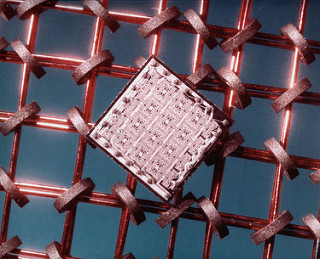
Original image: 64-bit Chip. By Steve Jurvetson [Image license]
